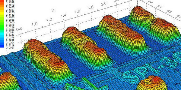
Solder Paste Inspection Process: Unlocking Precision for Printed Circuit Boards
Our Solder paste inspection process equipment empowers you to detect flaws swiftly and accurately, ensuring pristine printed circuit boards. Available in North Carolina and worldwide through our expert partners, our systems offer a comprehensive solution for enhancing your manufacturing quality.
Overview of Solder Paste Inspection Process Capabilities
ASC International, the global leader in Solder paste inspection process, brings you cutting-edge solutions for maximizing your PCB manufacturing efficiency. Our systems leverage advanced optical technologies, including microscopes and lasers, to provide unparalleled accuracy in flaw detection.
The human eye has limited ability to discern flaws below 50μm. Our systems employ sequential magnification to pinpoint imperfections precisely, minimizing the time and effort required for manual inspection.
The ASC International Solder Paste Inspection Process System
Our Solder paste inspection process System revolutionizes flaw identification with its unparalleled combination of AOI-detected position data, high magnification, and wide-field selection. Using this system:
- Identify flaws swiftly and capture images instantly.
- Utilize mouse scrolling for seamless zooming, saving substantial labor costs.
Technical Specifications
- Imaging Capabilities: High-resolution imaging with low noise and excellent image quality, capturing every detail for intricate analysis.
- Conical Convergence and Illumination: Circular, high-brightness illumination eliminates blind spots and enhances visual inspection effectiveness.
Customized System Configuration
Our Solder paste inspection process systems can be tailored to your specific needs:
- Dedicated Stations: Designated stations for specific tasks, optimizing workflow.
- Flexible Configurations: Customizable setups for varying board sizes and inspection requirements.
Case Study: Success in North Carolina
A leading Electronics Manufacturing Services company in North Carolina faced challenges with manual solder paste inspection. ASC International’s system:
- Reduced inspection time by 50%.
- Eliminated human error, ensuring consistent quality.
- Increased production efficiency and customer satisfaction.
Key Considerations
- Camera Resolution: Higher resolution cameras capture finer details.
- Magnification Range: Select systems with the appropriate magnification range for your application.
- Illumination: Optimal illumination ensures clear and accurate images.
Benefits
- Enhanced Detection: Precise flaw detection improves product quality and reliability.
- Cost Savings: Automated inspection minimizes labor expenses.
- Increased Efficiency: Swift inspection speeds up production time.
Future Outlook
- AI and Machine Learning: Integration of AI/ML algorithms for automated defect classification.
- Advanced Illumination Techniques: Enhanced illumination technologies for improved image quality and flaw detection.
Expansive Summary:
Our comprehensive Solder paste inspection process solutions empower you to achieve unparalleled precision in your PCB manufacturing process. From high-resolution imaging and conical convergence to customized system configurations and innovative technologies, ASC International provides the tools you need to optimize quality control, reduce costs, and enhance efficiency.
Whether you’re in North Carolina or anywhere worldwide, our team of experts and proven case studies demonstrate our commitment to delivering exceptional value. Embrace the future of Solder paste inspection process with ASC International and unlock the potential for pristine printed circuit boards.


