AOI Technology
Automated Optical Inspection (AOI)
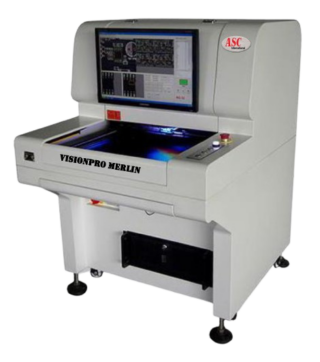
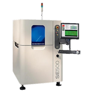
AOI Systems provided by ASC International employ a number of unique and innovative lighting technologies and algorithm-based tools to eliminate escapes and reduce false call rates.
Image Matching
The high-resolution color camera captures the image of the components and then through a series of algorithms determines if the components are acceptable based on features such as image size, position, brightness, and pasting angle.
Statistical Image Modeling
Images are compared to a large library of master images collected during the “learn mode” in order to provide as many possible variations as associated with the component manufacturing process.
Optical LED Analytics
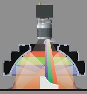
Using a high-resolution color camera along with an LED lighting scheme and RGB-W principles, images are analyzed based on reflection, refraction, and angular reflection characteristics.
SPI Technology
Solder Paste Inspection (SPI)
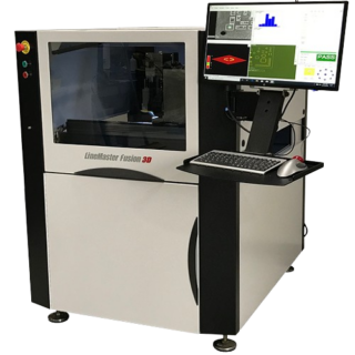
The core technologies for ASC International’s Solder Paste Inspection systems are laser-based or structured white light moiré interferometry.
Laser-Based Technology
How does laser-based technology work?
Utilizing the core principles of laser triangulation, a laser stripe is projected at a specific angle to the imaging camera. As the laser moves across the surface, a string of data is automatically collected from the centroid of the laser stripe generating a differential height reading from the base surface to the overall surface of the solder paste deposit. Single laser stripe SPI systems provide accurate and reliable height characteristics along with 2D cross-sectional profiles whereas laser scanning sensor SPI systems can provide accurate and reliable height, area, and volume characteristics with more complete 3D profiles for advanced qualitative analysis. Laser Technology based SPI systems are typically require less of an investment, yet still provide sufficient data results for basic height, width and area measurements.
There are over 40 variables associated with the solder paste printing process. The key to a successful yield improvement strategy is understanding these variables and creating a proactive approach to process control.
Structured White Light Moiré Interferometry
How does structured white light moiré interferometry technology work?
A known light pattern is projected onto a surface with the image being transferred to a high-resolution camera. On a flat surface, the projected pattern image appears to be undistorted to the camera. On a contoured surface such as a freshly printed circuit board, the pattern will follow the height variations from the surface to the solder deposits and these images will appear distorted to the camera. The distorted image is compared with the undistorted image and the difference is directly related to the height of the contoured object at every pixel. Pixel-by-pixel data replication as provided by this technology offers the most accurate and reliable method for obtaining true 3D, volumetric measurements critical to your overall screen print process strategy.
There are over 40 variables associated with the solder paste printing process. The key to a successful yield improvement strategy is understanding these variables and creating a proactive approach to process control.
Process Control Strategies
Recognized Leader in Quality Inspection Solutions.
Your Partner for Improved Yields & Process Control
Show your customers you are a quality-focused manufacturing company… invest in AOI and SPI.
Manufacturing quality into your products begins at the point when proactive process control strategies are implemented. Asking yourself the questions, “Why inspect components” and “Why inspect solder paste” provides the valuable information necessary to justify the need for these critical process improvement tools.
Save Time & Expense
- Improve yields, uptime and throughput
- Improve Quality
- Improve process control and operational efficiencies
- Establish repeatable and verifiable standards
- Reduce training time and resource needs
- Reduce rework costs
- Manufacturing facilities worldwide are significantly improving yields, quality and operational efficiencies using ASC International’s systems for automated optical inspection (AOI), solder paste inspection (SPI) and coordinate measurements (CMM).
Why Inspect Components?
Component placement inspection has become even more critical over the past decade due to package sizes getting smaller and smaller. The key to a successful yield improvement strategy is understanding these placement defects and creating a proactive approach to process control.
Why Inspect Solder Paste?
There are over 40 variables associated with the solder paste printing process. The key to a successful yield improvement strategy is understanding these variables and creating a proactive approach to process control.
Why Inspect?
Learn more about the benefits of inspecting solder paste and components.
ASC International’s Role In Streamlining Electronics Production Through SMT Inspection
At ASC International, we understand that speed and quality go hand in hand within the electronic manufacturing industry. While assembling complex, highly functional electronic devices requires flawless SMT automated optical inspection, high-volume manufacturing relies on advanced, productivity-enhancing solutions.
That is why, as leaders in our field, we provide the advanced solutions required to ensure high level of precision. Our innovative SMT inspection services enable businesses to achieve excellence and uphold high standards across their production processes.
We Drive Excellence with SMT Automated Optical Inspection (AOI)
Our inspection services in SMT manufacturing involve AOI, or Automated Optical Inspection, to further improve efficiency and accuracy in electronics production. AOI systems use high-resolution cameras and sophisticated algorithms to take and analyze images of components. The systems confirm that components are correctly positioned, sized, and oriented perfectly to specification. It is a careful check that helps detect defects at an early stage of production, reducing the possibility of defects reaching the final product stage.
AOI technology ensures the reduction of false call rates for manufacturers by providing them with specific and actionable feedback for continuous improvements in production. The fact is valued at ASC International that identifying one defect early actually equates to less downtime and fewer production stoppages. At ASC International, we aim to assist you in your smooth lines by continuing to deliver products that meet or surpass the highest possible quality standard.
Our Expertise in Solder Paste Inspection (SPI)
We also manufacture Solder Paste Inspection, a high-tech industry for checking the quality of solder paste applied to PCBs. Through advanced technologies ranging from laser-based measuring systems to Structured White Light Moiré interferometry, the company provides in-depth detail of solder paste deposits to give the exact required height, surface area, and volume that characterize good soldering.
Our SPI systems are specifically designed to determine discrepancies in paste application, right down to every detail, with a view toward the quality and reliability of the end product. Solder paste brings more than 40 variables into a process, whereas our inspection technology offers enhanced, proactive methods for process control: yields go up while expensive rework goes down.
Our Commitment to Quality and Customer Satisfaction
At ASC International, we are driven by quality and customer satisfaction. We understand that every product you manufacture is a reflection of your brand. We take pride in helping maintain the highest quality standards throughout your manufacturing process. From the first inspection to the final piece, we make sure every stage contributes to a superior result.
The cooperation with our company will greatly help develop and optimize production lines, especially when discussing accessing advanced technologies along with a close team of experts in that area. Our approach to SMT inspection follows a system supporting defect detection, yet it is based on process optimization. The results are innovative end products faster and more efficiently delivered.
Ensuring Precision and Efficiency in Electronics Production
ASC International smoothes out electronics production through our state-of-the-art SMT inspection services. Every process is done with guaranteed precision, quality, and efficiency due to using AOI and SPI technologies. We will always be there to assist manufacturers in their quest for optimum yields, cost reduction, and maintenance of operational excellence. By having ASC International as your partner, you will be assured that your products will meet the highest quality standards at all times.
Get in Touch with Us!
Ready to streamline your electronics production? Contact ASC International today to learn more about how our SMT inspection services can enhance your manufacturing processes. Our team of experts is here to provide tailored solutions that will help you achieve top-quality results and improve your production efficiency. Don’t wait—take the first step towards flawless production today!

