3D Solder Paste Inspection (SPI) Systems
Industry-leading 3D inspection technology for precise solder paste volume, height, and area measurement in PCB manufacturing
Our 3D SPI Systems
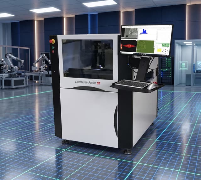
LineMaster Fusion 3D
High-speed inline 3D solder paste inspection with fully automatic measurement, eliminating operator errors and delivering outstanding repeatability at an affordable price.
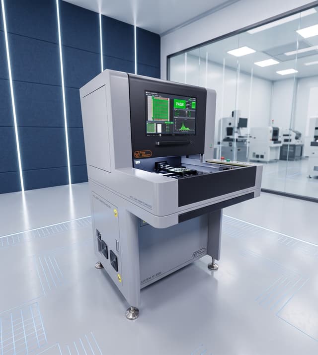
VisionPro HSi
High-speed portable benchtop 3D SPI system for the production floor. Accurate 3D measurements of paste pads, BGAs, and PCB features with excellent repeatability.
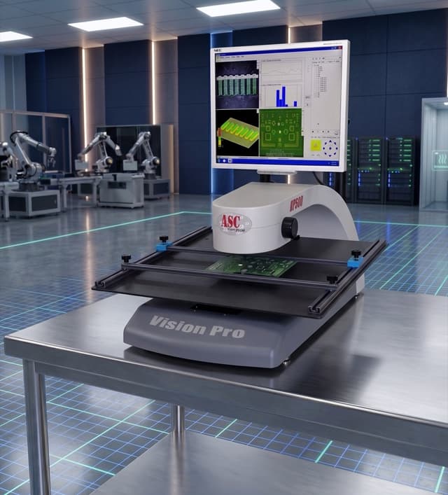
VisionPro AP500
ASC International's most popular VisionPro AP model — rugged benchtop 3D SPI with fully automatic measurement and minimal operator training required.
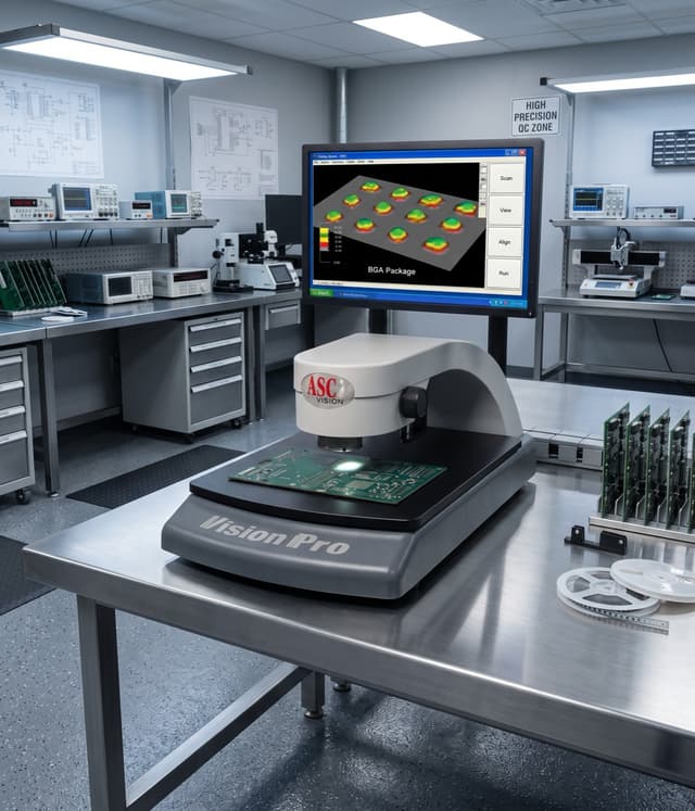
VisionPro SP3D
Laser-based benchtop SPI with reliable height, area, and volume measurements. Onboard SPC charting, custom data reports, and Windows 10/11 Pro via ASCan Ultra software.
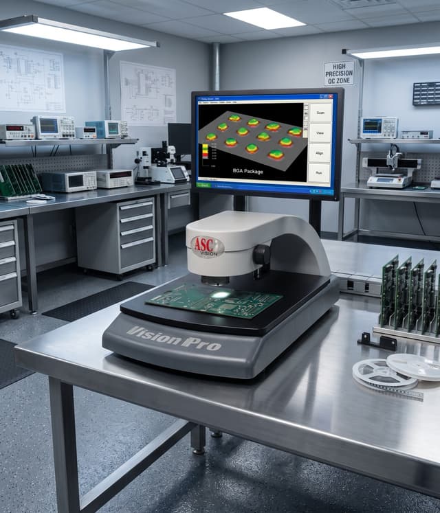
VisionPro M500
Advanced true 3D benchtop SPI with 0.48μm Z-resolution, 6.8μm lateral resolution, and a larger FOV sensor for superior paste measurement in demanding applications.
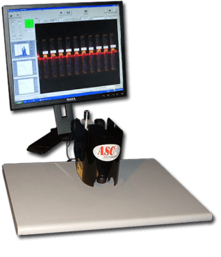
LaserVision SP3D Mini
Affordable laser-based 3D SPI delivering the same measurement capability as the VisionPro SP3D on a cost-optimized platform. Customer-supplied PC option available.
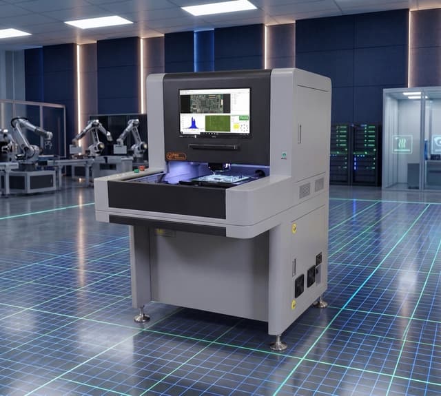
LineMaster DMI
Revolutionary dual-mode offline platform combining 3D SPI sensor technology with image-based AOI. Detects missing parts, bridging, polarity issues, and solder defects in a single pass.
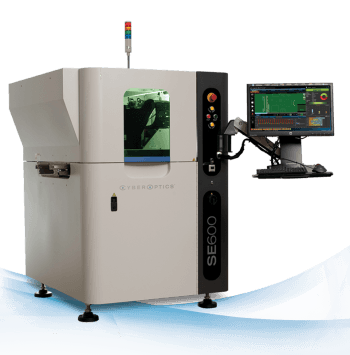
CyberOptics SE Series
Pre-owned high-speed inline 3D SPI from CyberOptics, the world's leading SPI supplier with 3,000+ installs. Award-winning CyberPrint OPTIMIZER software for closed-loop printer process control.
How the technology works, specifications and comparisons are below.
What is 3D Solder Paste Inspection?
3D Solder Paste Inspection (SPI) is a critical quality control process in electronics manufacturing that measures the volume, height, and area of solder paste deposits on printed circuit boards (PCBs) after the printing process and before component placement. Using advanced phase-shift measurement technology, 3D SPI systems achieve ±1μm height resolution and ±2% volume accuracy - far superior to traditional 2D inspection methods.
ASC International's 3D SPI systems use advanced optical technology and sophisticated algorithms to detect solder paste defects including insufficient volume, excessive volume, bridging, misalignment, and shape irregularities. Early detection of these defects prevents costly rework and improves overall manufacturing yield.
Why is SPI so important? Studies consistently show that 60-70% of all electronics manufacturing defects originate at the solder paste printing stage. Catching these defects with SPI - before expensive components are placed - reduces fix costs by 100x compared to finding defects at AOI ($0.50 vs $50) or in the field ($500+). This makes 3D SPI one of the highest ROI investments in PCB assembly.
Modern 3D SPI systems provide real-time statistical process control (SPC) and closed-loop feedback to solder paste printers, enabling automatic correction of offset and volume issues. This continuous improvement capability helps manufacturers achieve Six Sigma quality levels and meet stringent IPC Class 2 and Class 3 workmanship standards required for automotive, medical, and aerospace applications.
How 3D SPI Works: Step-by-Step Process
Board Loading
After solder paste printing, the PCB automatically transfers from the printer to the SPI system via SMEMA conveyor. The system reads the board barcode for traceability and loads the appropriate inspection program based on the board type.
Fiducial Detection & Alignment
High-resolution cameras locate fiducial marks on the PCB with sub-pixel accuracy. The system calculates board position and rotation, then aligns inspection coordinates to the actual board position, compensating for any misalignment from the printer.
3D Measurement
The system projects multiple structured light patterns onto the board surface. Phase-shift algorithms analyze pattern distortion to construct a complete 3D point cloud showing the exact topography of all solder paste deposits. This process captures millions of height measurements across the board in seconds.
Defect Analysis
Advanced algorithms calculate volume, height, area, and X/Y offset for each paste deposit. The system compares these measurements against programmed tolerances and flags any deposits outside specifications. It detects insufficient paste, excessive paste, bridging, offset, missing deposits, and shape irregularities.
Decision & Feedback
Based on inspection results, the system marks the board as PASS or FAIL. Real-time SPC charts track process trends (Cpk, X-bar, R-charts). Closed-loop feedback sends correction data back to the printer to automatically adjust stencil alignment or squeegee pressure. Failed boards can be routed to rework or scrap based on your process rules.
Data Logging & Reporting
All inspection data is logged to the database with board serial number, timestamp, and full measurement results. The system generates reports in PDF, CSV, or XML format and sends data to your MES/ERP system via IPC-CFX, OPC-UA, or REST API. This complete traceability supports ISO 9001, IATF 16949, and AS9100 quality requirements.
Return on Investment: Why 3D SPI Pays for Itself
Most manufacturers achieve 6-12 month payback on 3D SPI investment through defect cost reduction, scrap savings, and yield improvement.
Cost Savings
- Reduce rework costs by 50-80%
- Eliminate wasted components on bad boards
- Decrease field failures and warranty claims
- Reduce manual inspection labor
Quality Benefits
- Improve first-pass yield by 10-20%
- Achieve Six Sigma process capability (Cpk > 1.67)
- Meet IPC Class 3 quality requirements
- Complete traceability for ISO/AS9100 compliance
Real-World Example
A mid-size contract manufacturer producing 500 boards/day found that installing 3D SPI reduced their scrap rate from 3% to 0.5%. With average board value of $200, this saved $750,000 annually in scrap costs alone - paying back the SPI investment in just 4 months.
Read our complete SPI ROI guide →Key Features & Benefits
High Accuracy
Precise 3D measurement with ±1μm height resolution for accurate solder paste volume calculation
Fast Inspection Speed
High-speed inspection up to 85cm²/sec for maximum production throughput
Real-Time SPC
Statistical process control with trend analysis for continuous process improvement
Industry 4.0 Ready
Full factory integration with IPC-CFX, SECS/GEM, and custom API support
Flexible Configuration
Available in inline and offline configurations to fit your production line
Proven Reliability
34+ years of experience with more than 2,500 installations worldwide
3D SPI vs 2D SPI Comparison
Understanding the key differences between 3D and 2D solder paste inspection technologies
| Feature | 3D SPI (Recommended) | 2D SPI |
|---|---|---|
| Volume Measurement | Direct measurement (±2% accuracy) | Calculated (±10-15% accuracy) |
| Height Measurement | Direct measurement (±1μm) | Not available |
| Area Measurement | High accuracy | High accuracy |
| Bridging Detection | Excellent (3D profile analysis) | Limited (2D view only) |
| PCB Warpage Handling | Automatic compensation up to 3mm | Requires manual setup |
| Coplanarity Detection | Yes (full 3D measurement) | No |
| False Call Rate | < 1% (with proper setup) | 3-5% typical |
| Best For | Fine pitch, high reliability, Class 3 | Large pads, Class 1-2, budget constraints |
| ROI Timeframe | 12-18 months typical | 18-24 months typical |
Recommendation: 3D SPI is the industry standard for modern electronics manufacturing. The superior accuracy and lower false call rate result in better ROI despite higher initial cost. Read our detailed 3D SPI vs 2D SPI comparison guide.
Common Applications
SMT Assembly Lines
Critical quality checkpoint after solder paste printing, before component placement
High-Mix Production
Fast program changeover for facilities producing multiple PCB designs
Fine-Pitch Components
Precise inspection of 01005 components and ultra-fine pitch BGAs
Process Optimization
Data-driven printer optimization and maintenance scheduling
Technical Specifications
Measurement Performance
| Inspection Technology | Phase-shift 3D measurement with structured light projection |
| Height Resolution | ±1μm (0.00004") |
| XY Resolution | 10μm - 20μm configurable (0.0004" - 0.0008") |
| Repeatability | ±0.5μm (3σ) |
| Measurement Method | Non-contact optical measurement |
| Inspection Speed | Up to 85cm²/sec (13.2 in²/sec) |
Board Handling
| Board Size Range | 50mm × 50mm to 510mm × 460mm (2" × 2" to 20" × 18") |
| Board Thickness | 0.4mm - 6.0mm (0.016" - 0.24") |
| Board Weight | Up to 5kg (11 lbs) |
| Board Warpage Handling | Up to 3mm with automatic height compensation |
| Conveyor Type | Dual-lane SMEMA compatible |
| Transport Height | 900mm ± 20mm (35.4" ± 0.8") |
Inspection Capabilities
| Smallest Component Size | 01005 (0.4mm × 0.2mm / Metric 0402) |
| Minimum Pad Pitch | 0.3mm (0.012") |
| Defect Detection | Insufficient paste, excess paste, bridging, offset, shape defects, missing deposits |
| Measurement Parameters | Volume, height, area, X/Y offset, shape analysis |
| Fiducial Detection | Automatic recognition with sub-pixel accuracy |
Software & Integration
| Programming Methods | Auto-programming from CAD, teach mode, golden board |
| Communication Protocols | IPC-CFX, SECS/GEM, SMEMA, Modbus TCP/IP |
| Data Formats | Gerber (RS-274X), ODB++, GenCAD, IPC-2581 |
| Statistical Analysis | Real-time SPC, Cpk calculation, trend charts, control charts |
| Closed-Loop Feedback | Automatic printer adjustment, offset correction |
| Reporting | PDF, CSV, XML export with customizable templates |
| Traceability | Barcode/2D code reading, serial number tracking |
Environmental & Physical
| Machine Dimensions | 1200mm (L) × 1100mm (W) × 1450mm (H) |
| Machine Weight | Approximately 600kg (1,320 lbs) |
| Power Requirements | AC 200-240V, 50/60Hz, Single phase, 1.5kVA |
| Compressed Air | 0.5-0.7 MPa (73-100 PSI), clean dry air |
| Operating Temperature | 20°C - 28°C (68°F - 82°F) |
| Operating Humidity | 35% - 75% RH, non-condensing |
Need a Complete Specification Sheet?
Download our comprehensive PDF specification sheet with detailed technical diagrams, measurement examples, and integration guidelines.
Request Detailed SpecsWhy Choose ASC for 3D SPI
Open Architecture
IPC-CFX, SECS/GEM, works with any printer brand
Sub-Micron Repeatability
±0.5μm (3σ) proven in production environments
No Proprietary Data Lock-In
Export to CSV, XML, or any format you need
Direct Engineer Support
Talk to the people who built the system, not a call center
Evaluating SPI vendors? Read our SPI Vendor Comparison Guide or 2026 SPI Buyer's Guide.
Ready to Improve Your Solder Paste Process?
Contact our experts to learn how ASC's 3D SPI systems can reduce defects and increase yield in your production line